
.jpg) 1 hour ago
3
1 hour ago
3
Article content
Platform uses silicon wafer itself as the package and introduces a highly integrated approach to power system design across automotive, industrial, and AI data center markets

THIS CONTENT IS RESERVED FOR SUBSCRIBERS ONLY
Subscribe now to read the latest news in your city and across Canada.
- Exclusive articles from Barbara Shecter, Joe O'Connor, Gabriel Friedman, and others.
- Daily content from Financial Times, the world's leading global business publication.
- Unlimited online access to read articles from Financial Post, National Post and 15 news sites across Canada with one account.
- National Post ePaper, an electronic replica of the print edition to view on any device, share and comment on.
- Daily puzzles, including the New York Times Crossword.
SUBSCRIBE TO UNLOCK MORE ARTICLES
Subscribe now to read the latest news in your city and across Canada.
- Exclusive articles from Barbara Shecter, Joe O'Connor, Gabriel Friedman and others.
- Daily content from Financial Times, the world's leading global business publication.
- Unlimited online access to read articles from Financial Post, National Post and 15 news sites across Canada with one account.
- National Post ePaper, an electronic replica of the print edition to view on any device, share and comment on.
- Daily puzzles, including the New York Times Crossword.
REGISTER / SIGN IN TO UNLOCK MORE ARTICLES
Create an account or sign in to continue with your reading experience.
- Access articles from across Canada with one account.
- Share your thoughts and join the conversation in the comments.
- Enjoy additional articles per month.
- Get email updates from your favourite authors.
THIS ARTICLE IS FREE TO READ REGISTER TO UNLOCK.
Create an account or sign in to continue with your reading experience.
- Access articles from across Canada with one account
- Share your thoughts and join the conversation in the comments
- Enjoy additional articles per month
- Get email updates from your favourite authors
Sign In or Create an Account
or
Article content
Summary: onsemi today unveiled the Embedded Power Platform (EPP), redefining system power delivery through unprecedented power density and integration of multiple dies into a single silicon device. By jointly optimizing electrical, mechanical and thermal performance within a single architecture, EPP enables up to 3 – 5x higher power density compared with current solutions with a highly integrated approach to power system design. This helps customers reduce complexity while scaling for the increasing demands of AI infrastructure and electrification.
Article content
Article content
Article content
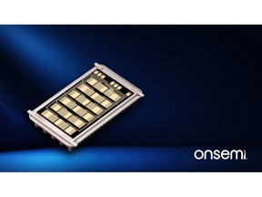
SCOTTSDALE, Ariz., Sept. 16, 2026 (GLOBE NEWSWIRE) — onsemi today unveiled the Embedded Power Platform (EPP), a breakthrough architecture that uses the silicon wafer itself as the foundation of the package and introduces a highly integrated approach to power system design. Designed as a scalable platform, EPP brings electrical, mechanical and thermal design together from the outset to help customers achieve higher power density, improve system performance and accelerate development in AI, electrification and autonomous applications.
Article content
By signing up you consent to receive the above newsletter from Postmedia Network Inc.
Article content
“For decades, the semiconductor and the package have been treated as separate technologies. EPP changes that by making the silicon itself part of the system architecture,” said Hassane El-Khoury, President and CEO of onsemi. “EPP brings together advanced semiconductor technologies, manufacturing and system-level optimization into a common architecture that can evolve alongside future innovations. This approach can redefine how power systems are built and create a new foundation for AI infrastructure, electrification and automation.”
Article content
Article content
What’s New: EPP reimagines the package from passive housing into an active contributor to system performance. By using the silicon wafer itself as the package, EPP enables the seamless integration and interconnection of silicon, silicon carbide (SiC) and gallium nitride (GaN) technologies within a highly integrated wafer-level architecture. Multiple devices, including FETs, drivers and controllers, can be embedded together in a single package and co-optimized for electrical, thermal and mechanical performance. This enables complete power-system co-design, allowing electrical, thermal and mechanical characteristics to be evaluated and optimized together from day one. The result is higher power density, improved system performance, reduced development complexity and faster time-to-market.
Article content
EPP also leverages onsemi’s standard 12-inch silicon wafer manufacturing capabilities, bringing key integration processes into the precision and control of the semiconductor fab. This applies mature semiconductor design tools, wafer-level manufacturing and advanced simulation capabilities to power-system integration, helping improve performance while accelerating innovation.
 English (US)